- 您现在的位置:买卖IC网 > Sheet目录1995 > HI3338KIBZ (Intersil)IC DAC 8BIT CMOS 16-SOIC
6
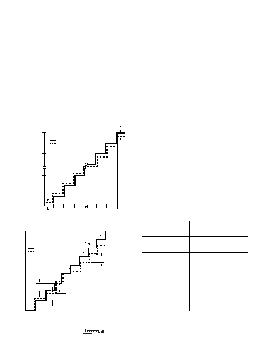
If the code into an 8-bit D/A is changed by 1 count, the
output should change by 1/255 (full-scale output-zero scale
output). A deviation from this step size is a differential
linearity error, see Figure 4. Note that the error is expressed
in fractions of the ideal step size (usually called an LSB).
Also note that if the (-) differential linearity error is less (in
absolute numbers) than 1 LSB, the device is monotonic.
(The output will always increase for increasing code or
decrease for decreasing code).
If the code into an 8-bit D/A is at any value, say “N”, the
output voltage should be N/255 of the full-scale output
(referred to the zero-scale output). Any deviation from that
output is an integral linearity error, usually expressed in
LSBs. See Figure 4.
Note that OFFSET and GAIN errors do not affect integral
linearity, as the linearity is referenced to actual zero and full
scale outputs, not ideal. Absolute accuracy would have to
also take these errors into account.
Dynamic Characteristics
Keeping the full-scale range (VREF+ - VREF-) as high as
possible gives the best linearity and lowest “glitch” energy
(referred to 1V). This provides the best “P” and “N” channel
gate drives (hence saturation resistance) and propagation
delays. The VREF+ (and VREF- if bipolar) terminal should be
well bypassed as near the chip as possible.
“Glitch” energy is defined as a spurious voltage that occurs
as the output is changed from one voltage to another. In a
binary input converter, it is usually highest at the most
significant bit transition (7FHEX to 80HEX for an 8-bit device),
and can be measured by displaying the output as the input
code alternates around that point. The “glitch” energy is the
area between the actual output display and an ideal one LSB
step voltage (subtracting negative area from positive), at
either the positive or negative-going step. It is usually
expressed in pV-s.
The HI3338 uses a modified R2R ladder, where the 3 most
significant bits drive a bar graph decoder and 7 equally
weighted resistors. This makes the “glitch” energy at each 1/8
scale transition (1FHEX to 20HEX, 3FHEX to 40HEX, etc.)
essentially equal, and far less than the MSB transition would
otherwise display.
For the purpose of comparison to other converters, the
output should be resistively divided to 1V full scale. Figure 5
shows a typical hook-up for checking “glitch” energy or
settling time.
The settling time of the A/D is mainly a function of the output
resistance (approximately 160
in parallel with the load
resistance) and the load plus internal chip capacitance. Both
“glitch” energy and settling time measurements require very
good circuit and probe grounding: a probe tip connector such
as Tektronix part number 131-0258-00 is recommended.
255/256
254/256
253/256
3/256
2/256
1/256
0
00
01
02
03
FD
FE
FF
= IDEAL TRANSFER CURVE
= ACTUAL TRANSFER CURVE
OFFSET
ERROR
(SHOWN +)
OUT
P
UT
V
O
L
T
A
G
E
AS
A
F
R
A
C
T
ION
O
F
V
REF
+
-
V
REF
-
GAIN ERROR (SHOWN -)
INPUT CODE IN HEXADECIMAL (COMP = LOW)
FIGURE 3. D/A OFFSET AND GAIN ERROR
0
00
OUT
P
UT
V
O
L
T
A
G
E
C
B
FROM “0” SCALE
INTEGRAL LINEARITY
ERROR (SHOWN -)
STRAIGHT LINE
TO FULL SCALE
VOLTAGE
INPUT CODE
= IDEAL TRANSFER CURVE
= ACTUAL TRANSFER CURVE
A = IDEAL STEP SIZE (1/255 OF FULL
B - A = +DIFFERENTIAL LINEARITY ERROR
C - A = -DIFFERENTIAL LINEARITY ERROR
A
SCALE -“0” SCALE VOLTAGE)
FIGURE 4. D/A INTEGRAL AND DIFFERENTIAL LINEARITY
TABLE 1. OUTPUT VOLTAGE vs INPUT CODE AND VREF
VREF+
VREF-
STEP SIZE
5.12V
0
0.0200V
5.00V
0
0.0195V
4.608V
0
0.0180V
2.56V
-2.56V
0.0200V
2.50V
-2.50V
0.0195V
Input Code
111111112 = FFHEX
111111102 = FEHEX
5.1000V
5.0800
4.9805V
4.9610
4.5900V
4.5720
2.5400V
2.5200
2.4805V
2.4610
100000012 = 81HEX
100000002 = 80HEX
011111112 = 7FHEX
2.5800
2.5600
2.5400
2.5195
2.5000
2.4805
2.3220
2.3040
2.2860
0.0200
0.0000
- 0.0200
0.0195
0.0000
-0.0195
000000012 = 01HEX
000000002 = 00HEX
0.0200
0.0000
0.0195
0.0000
0.0180
0.0000
-2.5400
-2.5600
-2.4805
-2.5000
HI3338
发布紧急采购,3分钟左右您将得到回复。
相关PDF资料
HI5628INZ
IC DAC 8BIT 125MSPS DUAL 48-LQFP
HI5660IBZ
CONV D/A 8-BIT 125MSPS 28-SOIC
HI5662/6IN
ADC DUAL 8-BIT 60MSPS 44-MQFP
HI5714/7CB-T
CONV A/D 8BIT 75MSPS 24-SOIC
HI5728/6INZ
DAC DUAL 10-BIT 60MHZ 48-LQFP
HI5731BIBZ
DAC 12BIT 100MHZ 5.2V 28-SOIC
HI5735KCBZ
CONV D/A 12BIT 80MSPS 28-SOIC
HI5741BIBZ
DAC 14BIT 100MHZ 5.2V 28-SOIC
相关代理商/技术参数
HI3338KIP
制造商:INTERSIL 制造商全称:Intersil Corporation 功能描述:8-Bit, CMOS R2R D/A Converter
HI33815
制造商:HARRIS 功能描述:*
HI3-381-5
制造商:未知厂家 制造商全称:未知厂家 功能描述:SPST Analog Switch
HI3-384-5
制造商:未知厂家 制造商全称:未知厂家 功能描述:DPST Analog Switch
HI3-387-5
制造商:未知厂家 制造商全称:未知厂家 功能描述:SPDT Analog Switch
HI3-390-5
制造商:未知厂家 制造商全称:未知厂家 功能描述:SPDT Analog Switch
HI33SD
制造商:未知厂家 制造商全称:未知厂家 功能描述:TRIAC|300V V(DRM)|3A I(T)RMS|TO-5
HI33SG
制造商:未知厂家 制造商全称:未知厂家 功能描述:TRIAC|300V V(DRM)|3A I(T)RMS|TO-5